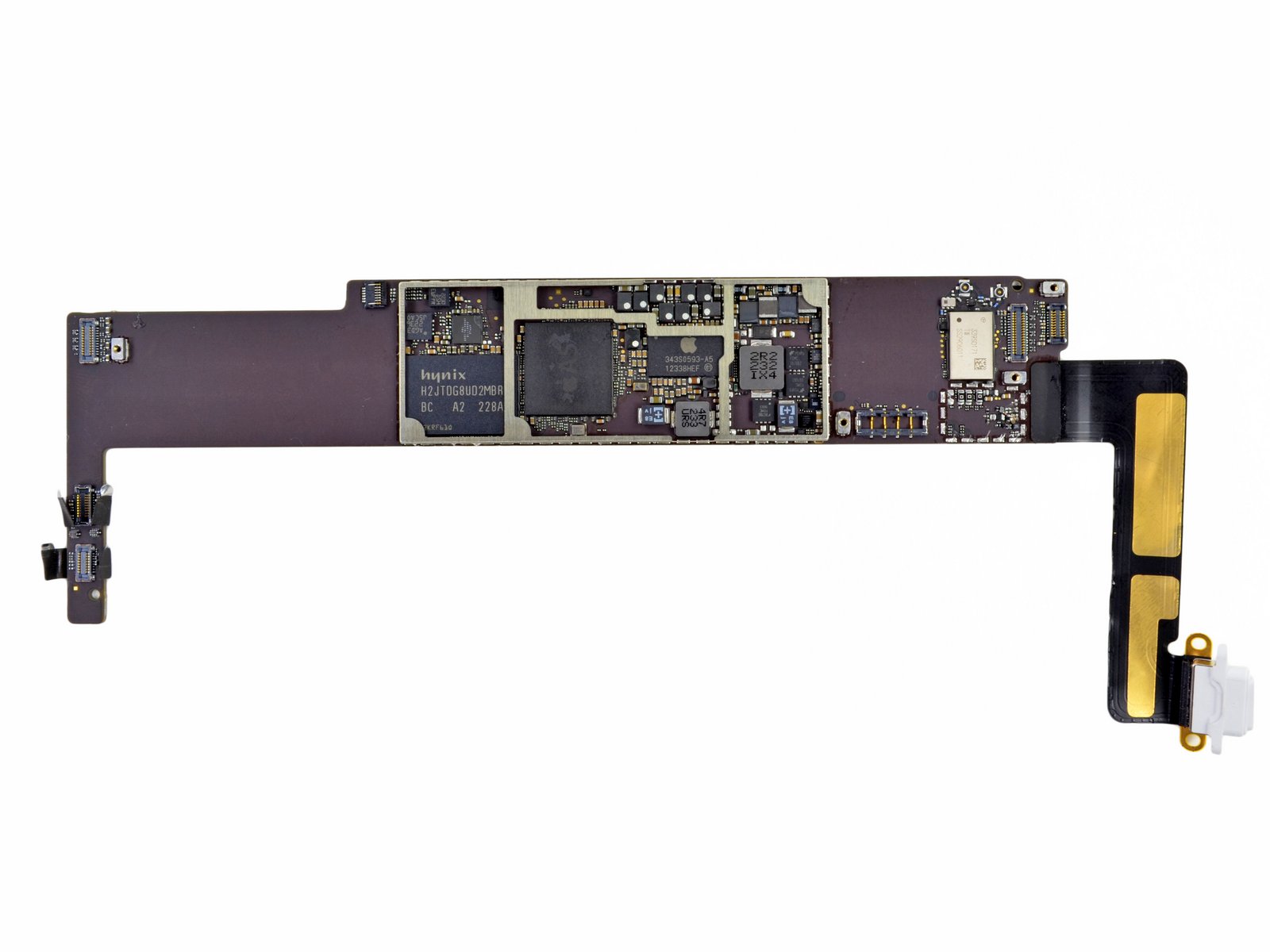
iPad Mini 4 Schematic Diagram: Inside Apple’s Design! Ipad air 2 schematic diagram download ipad air schematic diagram + pcb
Analyzing the intricate architecture of modern electronics requires detailed schematics and PCB layouts. These documents offer an invaluable insight into the device's functionality, component placement, and overall design, crucial for repair, reverse engineering, and understanding the device's electrical pathways. In the following sections, we delve into specific examples of iPad Air schematics and PCB layouts, highlighting key aspects and their significance.
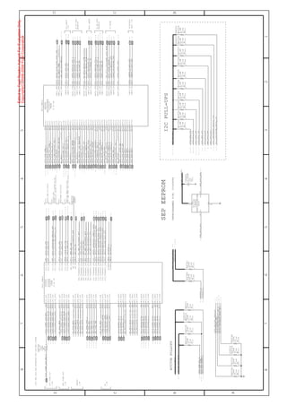
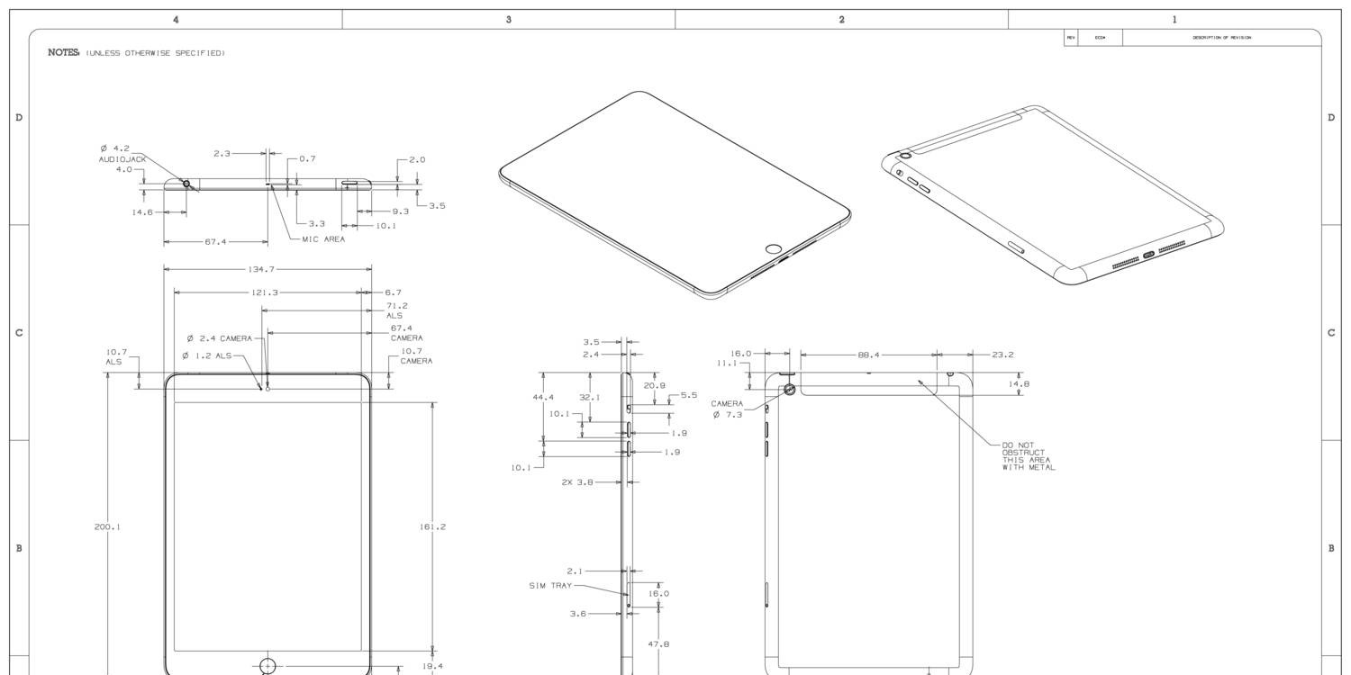
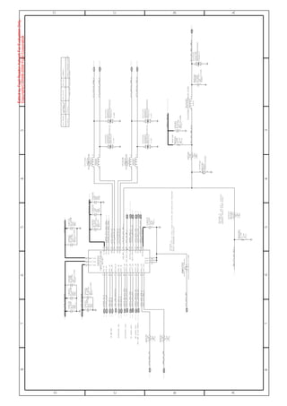
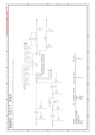
iPad Air Schematic Diagram and PCB Layout - Detail 1
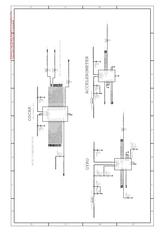
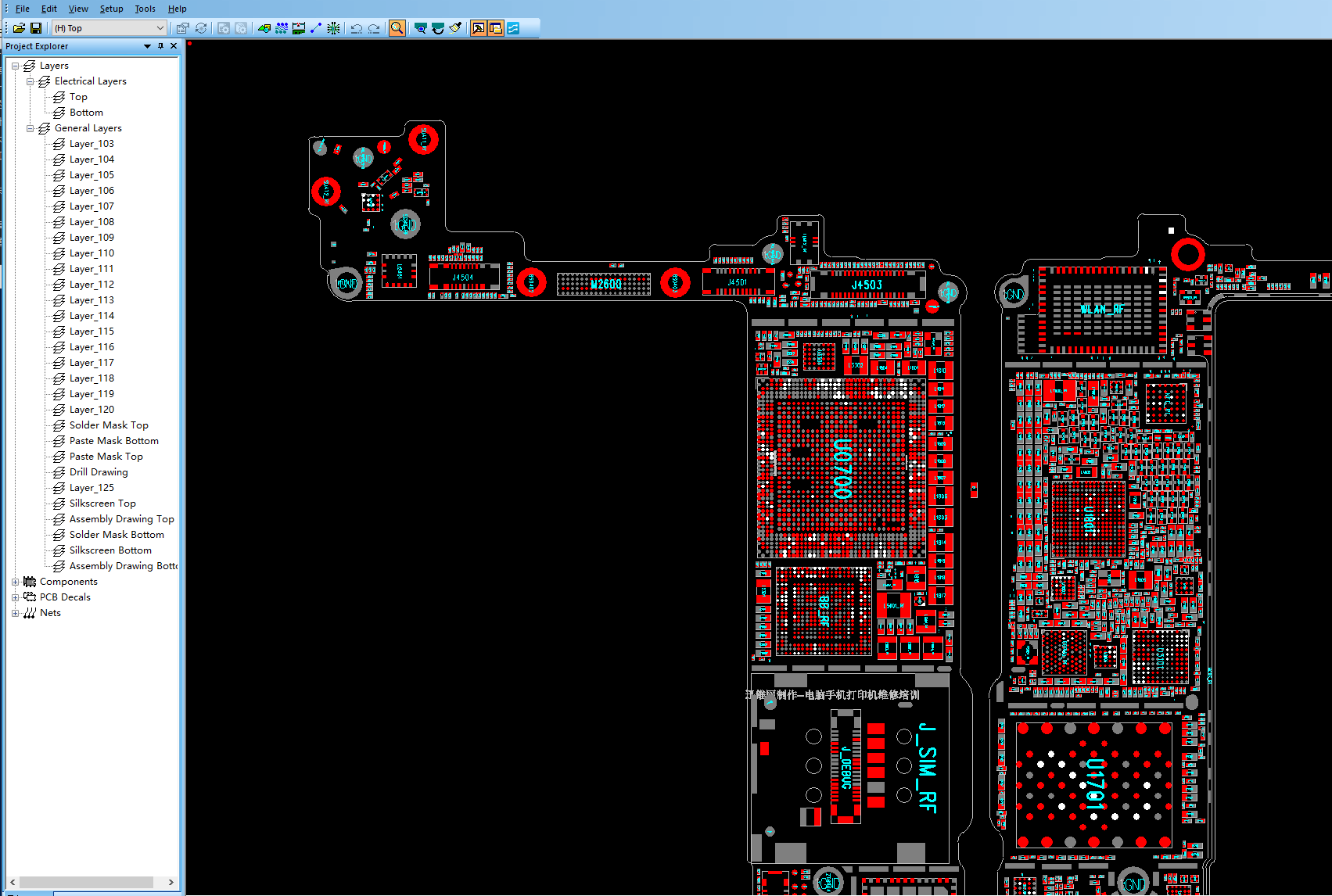
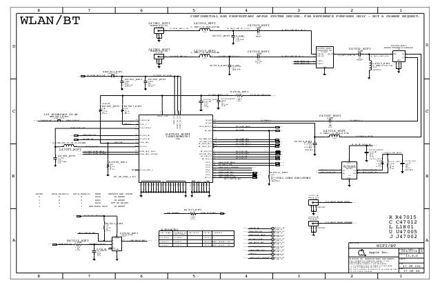
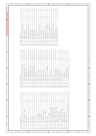
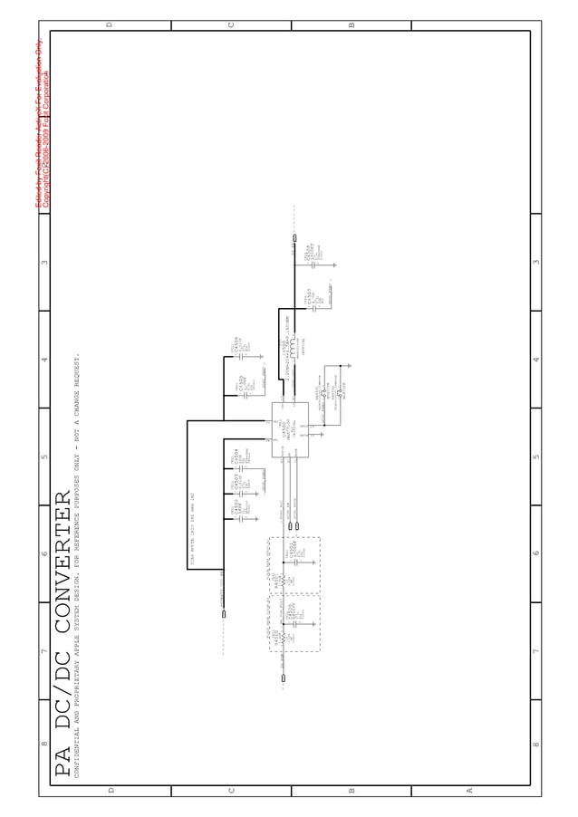
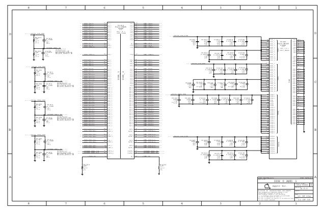
This image provides a snapshot of a section from an iPad Air schematic diagram and its corresponding PCB layout. The schematic illustrates the electrical connections between various components, showing how signals flow through the circuits. Understanding these signal pathways is paramount when troubleshooting issues, such as identifying short circuits, open connections, or faulty components. We can observe various components represented by their standardized symbols in the schematic diagram. Resistors, capacitors, inductors, diodes, and integrated circuits are all meticulously depicted, each with labeled values and connections. These labels are vital to ensure that any repairs or modifications are executed correctly. The PCB layout visually represents the physical arrangement of components on the printed circuit board. Each component is carefully placed to optimize signal integrity and minimize interference. Copper traces, visible as thin lines on the layout, connect the components and facilitate the flow of electricity. The traces are designed with specific widths and thicknesses to handle the required current. The meticulous design of the PCB layout is critical for the overall performance and reliability of the iPad Air. Any flaws in the layout, such as improper trace routing or inadequate grounding, can lead to signal degradation, electromagnetic interference, or even catastrophic failure. Analyzing this detailed view is a valuable exercise for engineers and technicians seeking to understand the intricate design principles behind modern electronics.
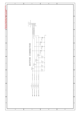
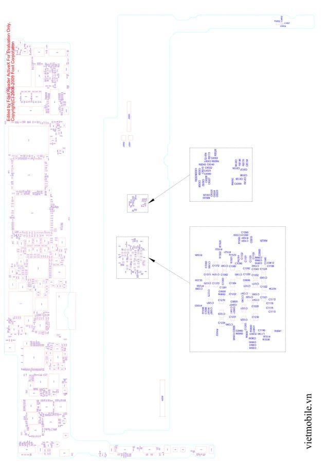
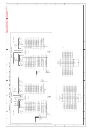
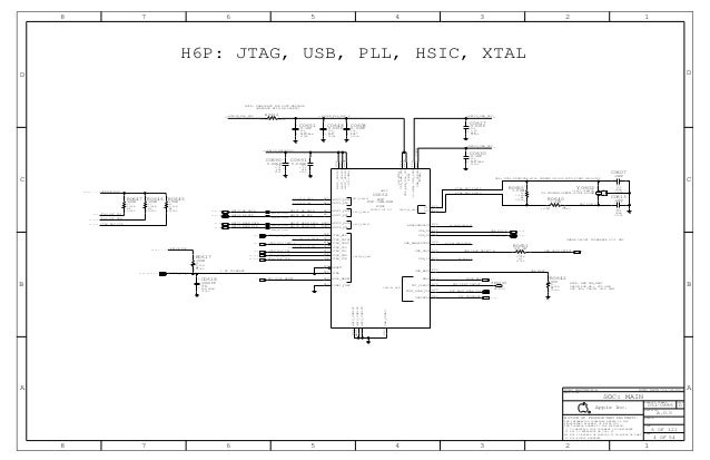
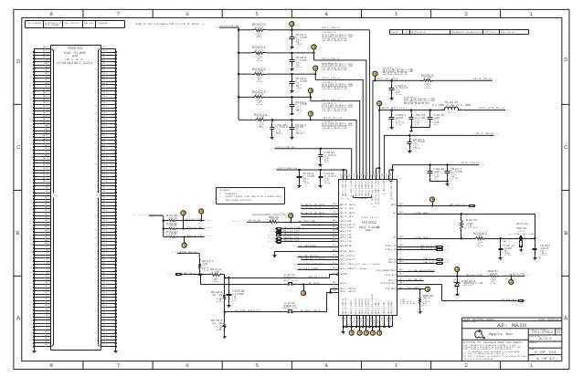
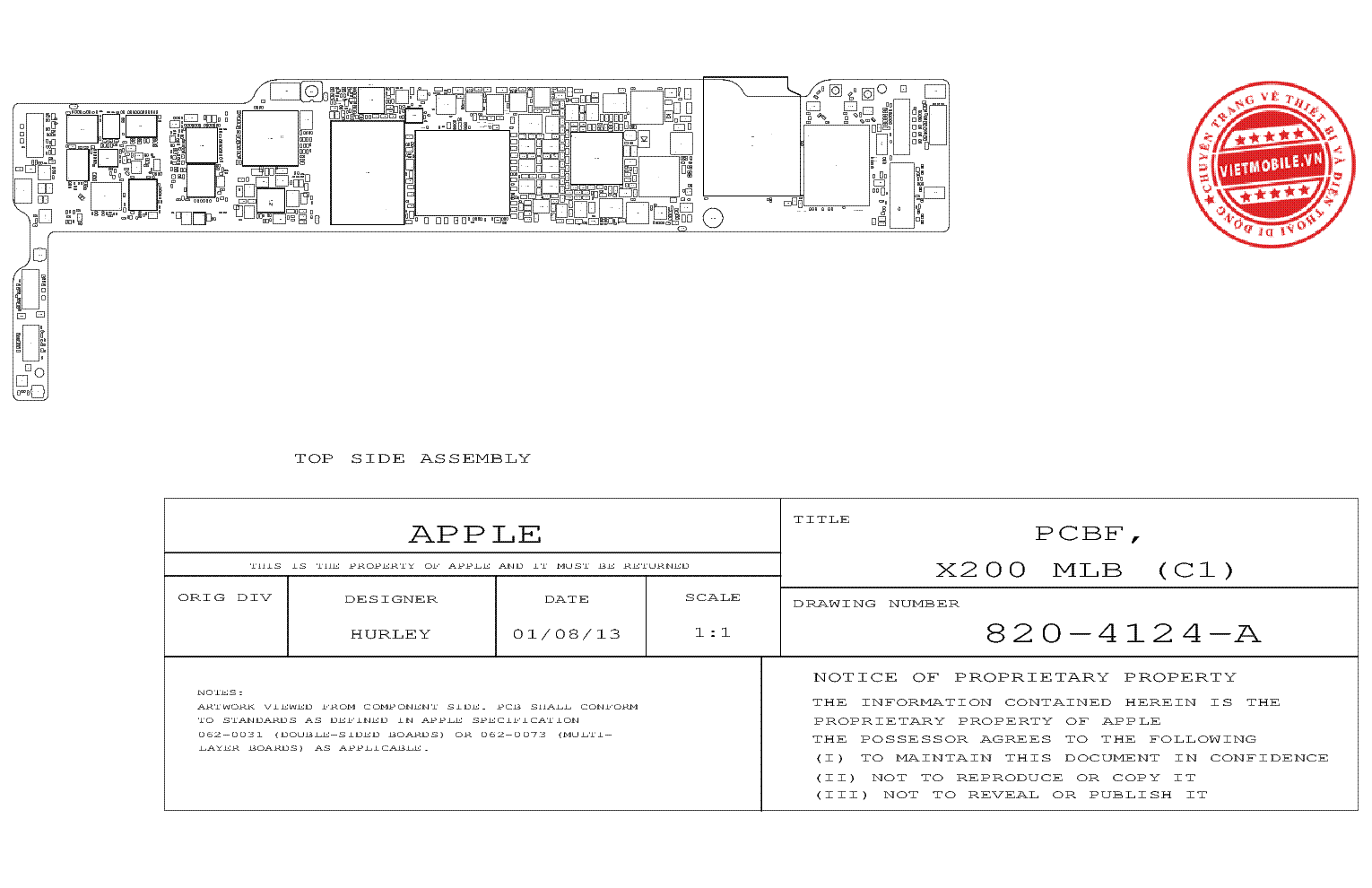
iPad Air Schematic Diagram and PCB Layout - Detail 2
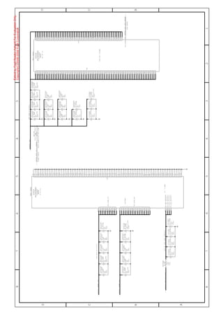
This image offers another perspective on the iPad Air's internal workings. The diagram showcases another portion of the device's complex circuitry. Once again, the schematic diagram provides a representation of the electrical connections between components, while the PCB layout illustrates the physical arrangement of these components on the board. The image shows a different section of the iPad Air's internal circuitry, allowing a broader comprehension of how different areas connect to each other. Here, we can see a concentration of smaller components and a denser network of copper traces. This might indicate a high-speed data processing or power management section of the device. Studying this specific area helps to better understand the functionality of this part. The schematic presents the individual elements involved, their values, and the nature of their interactions. The PCB layout reveals the optimized placement of these components on the printed circuit board. The proximity of components to each other, the width and routing of the copper traces, and the presence of grounding planes all contribute to the functionality. Furthermore, the specific component arrangement and placement will have been carefully considered to optimize heat dissipation, minimize signal interference, and ensure robust operation. Examining this image offers valuable insights into the design compromises and optimizations that engineers have to consider when developing complex electronic devices. Ultimately, these schematic diagrams and PCB layouts are important tools for understanding the intricacies of modern electronics, demonstrating the complexity and skill required to design such a device.
If you are searching about Ipad Air 2 Schematic Diagram Free Download Ipad Air Schematic Diagram you've came to the right web. We have 25 Images about Ipad Air 2 Schematic Diagram Free Download Ipad Air Schematic Diagram like Ipad Mini 4 Schematic Diagram Pdf Ipad Mini 4 Schematic Diagram, Ipad Pro 2 Schematic Diagram Ipad Schematics – Ecosdeltorbes and also Ipad 4 Schematic Diagram A1459 Ipad Mini 4 Schematic Diagram. Read more:
Ipad Air 2 Schematic Diagram Free Download Ipad Air Schematic Diagram
 ecosdeltorbes.net
 25+ Ipad 5 Schematic Diagram - AidanDorothy
 aidandorothy.blogspot.com
 Ipad Mini 4 Schematic Diagram Pdf / Ipad Mini Schematics Pdf Docdroid
 klr650-wiring-diagram43.blogspot.com
 Ipad Air 2 Schematic Diagram Download Ipad Air Schematic Diagram + Pcb
 ecosdeltorbes.net
 Ipad Pro 2 Schematic Diagram Ipad Schematics – Ecosdeltorbes
 ecosdeltorbes.net
 Ipad Air 2 Schematic Diagram Download Ipad Air Schematic Diagram + Pcb
 ecosdeltorbes.net
 Ipad Air 2 Schematic Diagram Download Ipad Air Schematic Diagram + Pcb
 ecosdeltorbes.net
 Ipad A2197 Schematic Diagram
 schematicdbisokontae.z21.web.core.windows.net
 Ipad 5 Schematic Diagram - ColennFraya
 colennfraya.blogspot.com
 Ipad Mini 4 Schematic Diagram Pdf / Ipad Mini Schematics Pdf Docdroid
 klr650-wiring-diagram43.blogspot.com
 Ipad Air 2 Schematic Diagram Free Download Ipad Air Schematic Diagram
 ecosdeltorbes.net
 Ipad Mini 4 Schematic Diagram Pdf / Ipad Mini Schematics Pdf Docdroid
 klr650-wiring-diagram43.blogspot.com
 Ipad Mini 3 Schematic Diagram Ipad Mini 2 Full Schematic Dia
 liturgia09d5glibguide.z14.web.core.windows.net
 Circuit Diagram App Ipad
 schematicfixtelsons.z22.web.core.windows.net
 Ipad 6 Schematic Diagram
 diagramlistsuable.z21.web.core.windows.net
 Ipad Air 2 Schematic Diagram Download Ipad Air Schematic Diagram + Pcb
 ecosdeltorbes.net
 Ipad Mini 4 Schematic Diagram Pdf / Ipad Mini Schematics Pdf Docdroid
 klr650-wiring-diagram43.blogspot.com
 Ipad Air 2 Schematic Diagram Free Download Ipad Air Schematic Diagram
ecosdeltorbes.net Ipad Air 2 Schematic Diagram Download Ipad Air Schematic Diagram + Pcb
 ecosdeltorbes.net
 Ipad Air 2 Schematic Diagram Download Ipad Air Schematic Diagram + Pcb
ecosdeltorbes.net Ipad 4 Schematic Diagram A1459 Ipad Mini 4 Schematic Diagram
 schematicvrcovice3ju.z14.web.core.windows.net
 Ipad Air 2 Schematic Diagram Free Download Ipad Air Schematic Diagram
 ecosdeltorbes.net
 Ipad Mini 4 Schematic Diagram Pdf Ipad Mini 4 Schematic Diagram
 ecosdeltorbes.net
 Ipad Air 2 Schematic Diagram Ipad Air 2 Design Changes Mean
 diagramfixemirb.z21.web.core.windows.net
 Ipad 4 Schematic Diagram Ipad Mini 4 Schematic
 diagramfixemirb.z21.web.core.windows.net
 Ipad pro 2 schematic diagram ipad schematics – ecosdeltorbes. 25+ ipad 5 schematic diagram. Ipad mini 4 schematic diagram pdf ipad mini 4 schematic diagram